UART COMMUNICATION BETWEEN FPGA AND MCU
The Universal Asynchronous Receiver/Transmitter (UART) protocol is one of the most popular serial communication protocols between digital devices for its simplicity to setup and versatility.
In this project, after a short recap of general theory, an example of UART communication between a Field Programmable Gate Array (FPGA) and a Microcontroller Unit (MCU) is discussed and analyzed. First, a VHDL script for transmitting characters to a PuTTY terminal is proposed. Then, the code is enhanced for handling UART reception too. In order to test the FPGA expected operation, an MCU is embedded programmed as counterpart.
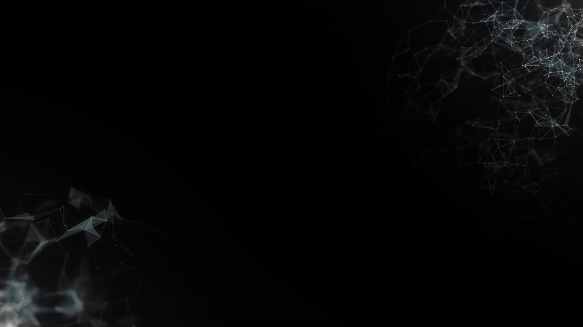
UART is a single-master / single-slave protocol, where one device is typically set up to communicate with only one partner by means of pair of data wires (commonly at 3.3 V or 5 V) and a common ground. UART communication between two devices can be full-duplex (if simultaneous communication to/from master/slave is guaranteed), half-duplex (if data can flow in just one direction at a time) or simplex (if only one-way communication is allowed). Data transmission takes place in the form of frames (see Fig.1), beginning with a start bit (SR) set to 0 (i.e. pulling the Tx line to ground). After the start bit, 5 to 9 info bits (IB) are transmitted, followed by an optional parity bit (PB) to check data consistency. Finally, one (or optionally two) stop bit (SP) set to 1 marks the end of the frame [1]. Of course, all of these parameters, as well as the baud rate [b/s], have to be known on both sides of the link. The necessity of agreeing the baud rate in advance is a consequence of the intrinsic asynchronous manner of the protocol, i.e. not providing a clock line from master to slave (unlike the USART case, for example).
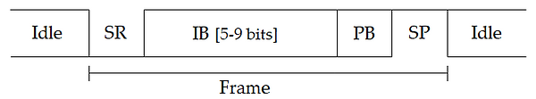
Fig.1 - UART protocol
In terms of hardware, the DE10-Lite [2] and Arduino UNO boards (shown in Fig.2) have been employed for the project. In particular, the DE10-Lite development board mounts an Altera MAX 10 FPGA and is equipped with GPIOs, buttons, switches, LEDs and a 50 MHz clock generator. The Arduino UNO board is based on an Atmel ATmega328P MCU and provided with GPIOs, memories and a 16 MHz crystal oscillator. Both can be simply powered and programmed via USB respectively by means of the dedicated Quartus Prime and Arduino IDE softwares in C and VHDL languages.
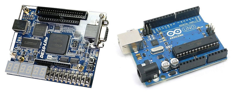
Fig.2 - DE10-Lite and Arduino UNO boards
Before establishing the UART communication between FPGA and MCU, another preliminary project (named UART-Chars) has been developed for testing the FPGA transmitting capability. In this case, the FPGA is programmed for automatically or manually sending sequences of ASCII characters (a sort of emulation of the C language printf function). As long as the SWT switch (see Fig.3) is in position '0', the FPGA stays in its automatic operation mode and its state machine (SM) can vary among states A, B and C. In particular, after being switched on, the FPGA starts in state A, in which it autonomously generates and sends once per second a message of 15 consecutive characters containing information about the current state and time (expressed in minutes, seconds and milliseconds), for example "A | 03:12:489\r\n". Then, each time the BTN0 button (see Fig.3) is pushed, the FPGA SM moves to next state (A→B, B→C or C→A). B and C are the same as state A except for the period between consecutive printings, which is increased respectively three and five-fold compared to the latter. Instead, when SWT is in position '1', the FPGA SM remains always in state D, where the generation and transmission of messages occurs only upon user request at each pressure of BTN0. Moreover, the VHDL code allows the user to change 3 parameters: the baud rate (by default at 100 kb/s), a flag for enabling/disabling the (even) parity bit and an integer scale factor (ScFct) for accordingly increasing automatic printing rates (e.g. if ScFct = 4, messages in states A, B and C are sent respectively every 250 ms, 750 ms and 1.25 s, instead of the standard 1 s, 3 s and 5 s).
The messages sent by the FPGA have been displayed on PC and checked by means of a TTL-to-USB converter (a model by DSD TECH mounting an FTDI FT232RL chip, shown in Fig.4) and the PuTTY free software, which, among other features, allows to establish a serial communication with the possibility of specifying all key UART parameters (e.g. baud rate, number of data bits per frame and parity bit pattern).
Examples of the aforementioned operation are depicted in Fig.5 and Fig.6a. The former is a simulation (obtained through an aimed tool inside Quartus environment) of the transmitted waveform for the first frames of a single message, whereas the latter is a screenshot of the messages received via PuTTY terminal (having set the baud rate to 100 kb/s, ScFct to 2 and enabled the parity bit check and scale factor as 2), whose configuration is reported in Fig.6b. In particular, Fig.6a shows how after about 32 minutes from its switching on, with SWT = '0' and never pressing BTN0, the FPGA SM holds in state A and sends messages every 500 ms. Then, after pushing BTN0 once and twice, state moves to B and then C, increasing printing periods 1.5 s and 2.5 s respectively. After pushing again BTN0, which moves SM back to A, SWT is toggled to '1' and printings start occurring only upon user request as explained above (in fact, it can be seen how printing time instants become no me periodic).
Fig.5 also highlights another important aspect of UART communication, namely that information bits are typically sent least significative bit (LSB) first.
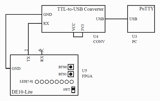
Fig.3 - UART-Chars project block diagram
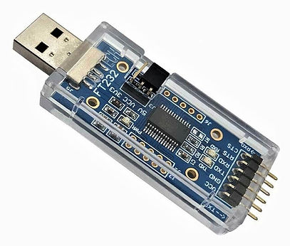
Fig.4 - TTL-to-USB converter

Fig.5 - UART-Chars project simulation

Fig.6 - (a) FPGA printings caught on PuTTY terminal, (b) PuTTY configuration page
After verifying the expected behaviour of the FPGA Tx section, the latter has been reused as starting point for the aforementioned main project (named UART-RTX), whose schematic drawn in Altium Designer is depicted in Fig.7. Here FPGA and MCU are programmed to communicate (both transmitting and receiving) each others via UART protocol. The operation of the UART-RTX project is the following:
-
Upon a pressure of BTN0, the FPGA is triggered to send the MCU a sequence of 4 bytes (in particular, if SWT is in position '1' the sequence is 0xD391A0C4, otherwise 0xD3D3D3D3).
-
The reception of any 4-byte message makes the MCU switch on all 4 LEDs (D1, D2, D3 and D4) and start an internal 2-second timer, which, once expired, enables the check of the received message.
-
If the latter matches the awaited value 0xD391A0C4, the MCU pulls out a pseudo-random value (calculated as the modulo 15 of an internal counter updated every 100 ms) representing the LED new configuration to be applied (e.g. 11d = 1011b causes D4 on, D3 off, D2 on and D1 on).
-
After updating the state of the LEDs connected to itself, the MCU forwards this value to the FPGA (in particular, as a message where the byte containing the value is repeated identical three times).
-
Upon the reception of three consecutive frames (all containing the same data byte), the FPGA updates its LED configuration in turn, so that the state of MCU and FPGA LEDs should be the same.
-
Instead, in case the received sequence from the FPGA does not match 0xD391A0C4 (e.g. if BTN0 is pushed while SWT is in position '0'), the MCU keeps all its LEDs on and forwards the same info to the FPGA.
-
In addition, a mechanism for flushing the Rx buffers of both FPGA and MCU are provided by simply pushing BTN1 and S1 respectively (see Fig.7).
The whole mechanism just explained is recapped graphically in Fig.8 thanks to a practical example, where the actual implementation of the schematic by means of breadboard and through-hole components is also shown.
In both directions the UART protocol foresees 8 info bits per frame, the presence of the (even) parity bit and one stop bit. By default, both baud rates are set to 100 kb/s, however these can be modified at will compatibly with the clock of the devices (anyway, from 500 b/s to 2 Mb/s the communication has been tested successfully). Moreover, the FPGA-to-MCU and MCU-to-FPGA baud rates can be set different from each other.
It is important to notice that while FPGA is able to establish a full-duplex communication (since transmission and reception are handled by separate and independent circuit sections), the same is not true on MCU side. In fact, the latter can only support half-duplex communication since it has available just one USART built-in interface, which cannot be used for transmitting and receiving at the same time.
Going in detail of the project schematic, since FPGA and MCU GPIOs work respectively at 3.3 V and 5 V, dedicated conversion networks are needed to guarantee the expected voltage levels, as shown in Fig.7. The down-conversion is obtained through a simple divider (R7 and R8), whereas the up-conversion by means of an npn-BJT (Q1) connected to a pull-up resistor (R5) and a 5 V reference from the MCU. The presence of R6 and R10 is useful respectively for limiting the base current and correctly anchoring its voltage to ground. Note that, since this network causes a logic reverse, the actual TX line outgoing from the FPGA (GPIO2) already foresees an additional not-operation in order to compensate it.
Concerning the FPGA hardware architecture, this is based on a mix of combinational and synchronous sequential networks. In particular, on Tx side the UART clock is generated from the built-in main one at 50 MHz, and then for each rising edge the proper bit of the message is sent over the TX output line. In addition, while transmitting the info bits, the sequential estimate of the parity bit is enabled (and the latter estimated with simple xor operations). Finally, in order to avoid undesired multiple transmissions due to a single pressure, a debouncer mechanism is foreseen for BTN0. On the other side, the overall Rx procedure is managed by a dedicated SM composed of six states:
-
1st state - Wait for a falling edge of the RX input line (GPIO6). If it occurs, move to next state, otherwise stay in 1st state.
-
2nd state - After waiting half bit period (optimal sampling instant), evaluate the RX line to check if it is still low (START bit). If so, move to next state, otherwise back to 1st state.
-
3rd state - At multiples of the bit period (i.e. the inverse the baud rate), sample the RX line and store the corresponding info bits into the internal Rx buffer. If the info bits are over, move to next state, otherwise stay in 3rd state.
-
4th state - After waiting another bit period, sample the RX line to read the parity bit. If the read value matches with the one calculated internally by the FPGA, move to next state, otherwise flush buffer and move back to 1st state.
-
5th state - After waiting another bit period, sample the RX line to check if it is high (STOP bit), If so, move to next state, otherwise flush buffer and move back to 1st state.
-
6th state - If all three frames have been received from MCU, check their consistency and update LEDs configuration, otherwise move to 1st state and wait for next frame.
A further simulation aimed at validating the receiving procedure just explained has been carried out. Its outcome is depicted in Fig.9 (for details about the meaning of the reported signals directly refer to the VHDL code).
In terms of MCU firmware, the proposed code intentionally does not employ any Arduino built-in functions, but directly exploit the ATmega328P potentiality and features [3] in order to show an example of microcontroller embedded programming. In particular, the firmware operation is based on three different interrupts, each handled through a dedicated interrupt service routine (ISR): one for the UART reception, one for the internal timer expiration, and one for the external interrupt (EXTI) generated by pressing S1 for flushing Rx buffer. For the assignments from MCU GPIOs to Arduino UNO pins (shown in Fig.7 as well), the official board schematic from manufacturer (reported and downloadable) has been considered.
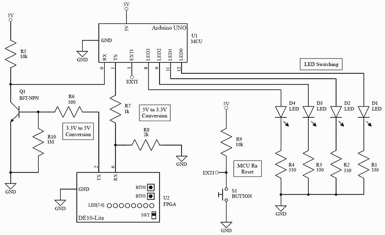
Fig.7 - UART-RTX project schematic
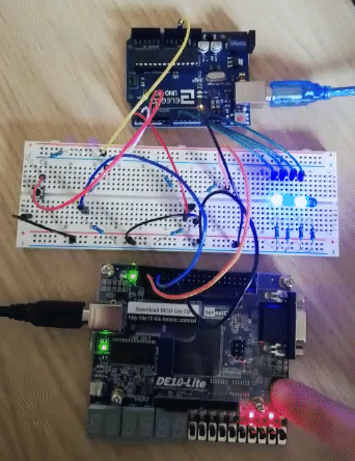
Fig.8 - Example of operation for the UART-RTX project

Fig.9 - UART-RTX project simulation
Below there is the link through which the aforementioned projects can be free downloaded. Regarding the Quartus projects, the main files to consider are the ones with extension .vhd, .qsf, .sdc and .vwf, containing respectively the essential VHDL code, the settings (e.g. the actual pin assignments), and the aforementioned simulations.
-
Download Quartus projects : UART-Quartus.zip
-
Download Arduino project : UART-RTX.ino
-
Download schematics : Schematics.zip
WARNING#1: FPGA and MCU codes have been developed respectively in Quartus Prime 18.1.0 (Lite Edition) and Arduino IDE 1.8.11. Therefore, their correct operation might not be assured with different softwares versions.
Last update : 19/04/2020
References
[1] Circuit Basics (link/a)
[2] DE10-Lite User Manual (link/b)
[3] ATmega328P Datasheet (link/c)